Baiyun Series
- Home
- Product Center
- Baiyun Series
Baiyun Series
TEM Camera
[Pioneering China’s Electron Microscopy Industry]
A Transmission Electron Microscopy (TEM) camera is a critical component used to capture and record images within a Transmission Electron Microscope. Installed in the imaging system of the microscope, it converts the electron signals—transmitted through the sample—into observable and storable images. The performance of a TEM camera directly affects image quality, resolution, and signal-to-noise ratio, making it an indispensable part of modern electron microscopy technology.
Against the backdrop of long-term reliance on imported technologies in this critical field, DRTem took the lead in independently developing high-performance, domestically produced TEM cameras—overcoming multiple core technological barriers. Our Baiyun Series products have been successfully applied in cutting-edge fields such as structural biology, advanced materials imaging, and semiconductor defect analysis. This marks a significant shift in China’s electron microscopy industry—from “usable” to truly “advanced” in core component innovation.
What are Indirect Electron Detection Cameras?
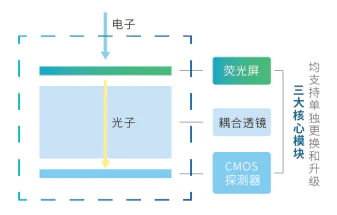
Indirect electron detection cameras are among the most traditional and widely used types of electron microscopy cameras. Their structure typically includes the following components: a scintillator screen, a prism or fiber-optic coupler, and a CCD or CMOS detector. The imaging process consists of the following steps:
1. The electron beam from the transmission electron microscope strikes the scintillator screen, converting the electron signal into a light signal.
2. The generated light signal is transmitted via an optical system (such as a lens or fiber-optic coupler).
3.The CMOS or CCD detector receives the transmitted light signal and converts it into a digital image.
Architecture and Imaging Workflow

Key Advantages and Application Scenarios
- Mature Technology: Indirect electron detection has a long history of development, characterized by well-established manufacturing processes and a relatively low cost.
- Signal Conversion Process: As the electron signal must be converted into a light signal, some signal loss and noise may be introduced. However, it still meets the requirements for standard high-resolution imaging.
- Widely used in materials science, biology, medicine, and industrial inspection. This technology is well-suited for routine characterization and high-resolution imaging of material samples, as well as imaging of negatively stained biological specimens and tissue sections.
- With its low cost, broad compatibility, and flexible deployment, it meets the needs of most scientific research environments.


